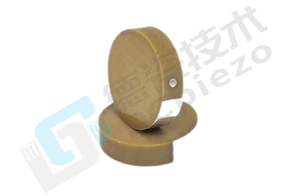
Circular Piezoelectric Ceramic Chip
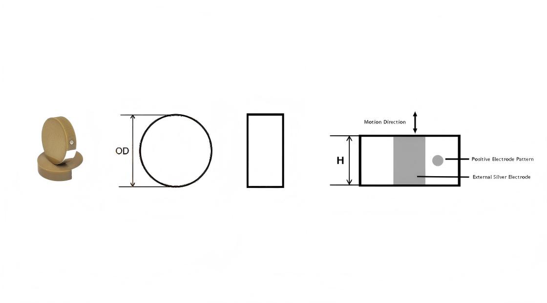
A high-precision multi-layer stacked piezoelectric core component designed for low-voltage actuation, delivering micron-level linear displacement and rapid response. Its circular multi-layer ceramic-electrode stacking structure features printed external electrodes and full-edge ceramic insulation with a "dot" polarity marker for reliable installation. Widely used in optical focusing, ultrasonic transduction, precision automation, and MEMS systems, it provides efficient electromechanical conversion for miniaturized, low-power devices.

Circular Piezoelectric Ceramic Chip

Circular Piezoelectric Ceramic Chip
Combining low-voltage operation, high-accuracy displacement, and compact design to serve as an ideal core driver for microsystems and precision equipment. As specialized manufacturers, we deliver reliable, rapid-response solutions through stringent process control and customization, empowering innovation in optics, medical, and industrial fields.
Structural Design
● Multi-Layer Cross Stacking: Ultra-thin piezoelectric ceramic layers alternating with internal electrodes, with external electrodes printed on both sides. Standard 2mm thickness (1-10mm customizable) achieves 0.1% thickness-to-displacement ratio and >98% linearity.
● Full-Edge Insulation: Moisture/leakage-proof ceramic encapsulation on the perimeter, featuring a side "dot" polarity marker for error-free installation.
● Precision Sizing: Standard 5.0mm/8.0mm diameters (customizable) with <±5μm flatness for miniaturized device integration.
● Modular Flexibility: Operate as single chips or stacked arrays to extend displacement/force output for diverse applications.
Material Properties
● High-Sensitivity Piezoelectric Ceramic: Modified PZT-based material with d33≥480 pC/N, achieving <5% energy loss and superior electromechanical coupling.
● Low-Impedance Electrodes: Ag-Pd alloy internal electrodes and Ag-printed external electrodes (resistivity <0.25Ω·cm) support 0V~150V driving and kHz-level operation.
● Precision Machining: Laser-cut with ±0.1mm diameter tolerance and Ra<0.2μm surface roughness for optimal energy transfer.
Core Advantages
● Ultra-Low Voltage Drive: Operates at 0V~75V/0V~100V/0V~150V with 120N/mm² force density, ideal for battery-powered devices.
● Micron-Level Control: Nanometer resolution per chip, extendable to tens of microns via stacking, with <0.1% repeatability.
● Millisecond Response: <100μs electromechanical response enables high-frequency vibration control and real-time adjustments.
● Environmental Durability: Full-ceramic encapsulation withstands humidity/aging, operable at -25°C~130°C with >1×10⁸ cycle life.
Typical Applications
● Optical Alignment: Endoscopic lens focusing actuation, laser cavity dynamic tuning.
● Ultrasonic Systems: Ultrasonic welding transducers, medical ultrasound probe transducers, sonar emitters.
● Industrial Automation: Precision valve micro-actuation, semiconductor packaging force feedback.
● MEMS: Micro-sensor excitation, microfluidic chip diaphragm pumps.
● Consumer Electronics: Wearable haptic feedback, micro-speaker diaphragm drives.
Quality Commitment
● Full-Process QC: Automated thickness/flatness inspection from tape casting to sintering, 100% polarization and displacement testing.
● Customization Expertise: Tailored diameters, thicknesses, voltage ranges, and force/displacement curves with prototypes in 5 business days.
● Technical Support: Driver circuit co-design, installation stress simulation, dynamic optimization, and 24/7 consultation.
