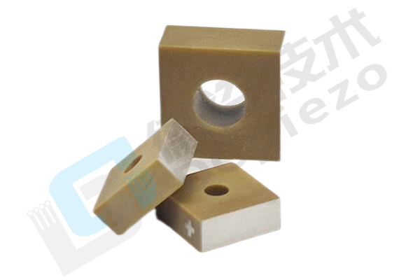
Square Central-Bore Piezoelectric Ceramic Chip
A core piezoelectric component engineered for high-dynamic precision actuation, featuring a multi-layer ceramic-electrode cross-stack structure with a central through-hole. This design achieves sub-nanometer displacement resolution and microsecond-level response. Alternating ultra-thin piezoelectric ceramic layers (dozens to hundreds) and internal electrodes are encapsulated by ceramic insulation on all sides, while the central bore enables preload mounting or optical/fluidic channel integration. Ideal for optical alignment, semiconductor processing, and ultrasonic systems, it serves as a compact, high-reliability core for miniaturized precision applications.

Square Central-Bore Piezoelectric Ceramic Chip

Square Central-Bore Piezoelectric Ceramic Chip
Redefining high-dynamic precision performance through multi-layer stacking and central bore innovation. As specialized manufacturers, we deliver highly consistent, rapid-response core components via material optimization and precision processes, advancing breakthroughs in optics, semiconductors, and ultrasonic technologies.
Structural Design
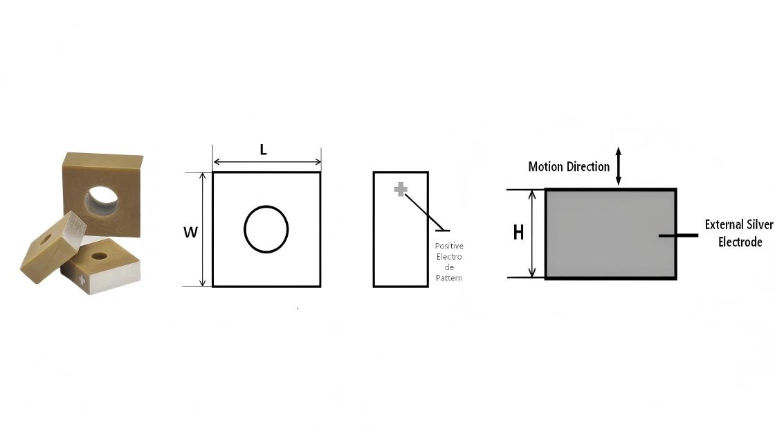
● Multi-Layer Cross Stacking: Alternating ceramic and internal electrode layers with external electrodes printed on both sides. Customizable stack thickness (standard: 2mm/3mm) achieves 0.1% thickness-to-displacement ratio and >99% linearity.
● Central Through-Hole: Custom-diameter bore for mechanical preloading or optical/fluidic integration, featuring smooth inner walls (Ra<0.1μm).
● Perimeter Insulation: Ceramic insulation layers on all sides for moisture and leakage protection, with "+/-" polarity markers to prevent misinstallation.
● Interface Flexibility: Available as bare chips or with bonded wires (Au/Cu) for soldering/spring-contact integration.
Material Properties
● High-Activity Piezoelectric Ceramic: PZT-based material with d33≥550 pC/N, high-temperature sintered for dense structure and long-term stability.
● Low-Loss Electrodes: Ag-Pd alloy internal electrodes and Ag-printed external electrodes (resistivity <0.2Ω·cm) support kHz-level driving with minimal thermal rise.
● Precision Machining: Flatness <±5μm, bore concentricity error <3μm, and optical-grade surface finish.
Core Advantages
● Sub-Nanometer Resolution: 0.1nm displacement resolution for ultra-precision positioning and micro-force control.
● Microsecond Response: <50μs electromechanical response enables high-frequency dynamic operations (vibration damping, fast valving).
● Compact Reliability: Full-ceramic adhesive-free structure with moisture/aging resistance and >1×10⁸ cycle life.
● Customization Ready: Tailored bore sizes, stack thicknesses, and electrode configurations for specialized integrations.
Typical Applications
● Optical Alignment: Laser beam stabilization apertures, adaptive mirror preload actuation.
● Semiconductor Tools: Wafer probe station micro-positioning, lithography mask nano-alignment.
● Ultrasonic Systems: High-frequency transducer arrays, microfluidic valve actuation.
● MEMS Devices: Micro-actuator drives, robotic joint displacement feedback.
● Research Instruments: STM tip actuation, cryogenic nano-positioning modules.
Quality Assurance
● Full-Process QC: Laser-monitored layer thickness/flatness, 100% high-voltage polarization and displacement testing.
● Rapid Prototyping: Custom bore (0.5-5mm), thickness (1-10mm), and electrode layouts (single/dual) with sampling proposals within 5 business days.
● Technical Support: Dynamic performance curves, installation stress analysis, driver circuit matching, and 24/7 consultation.
