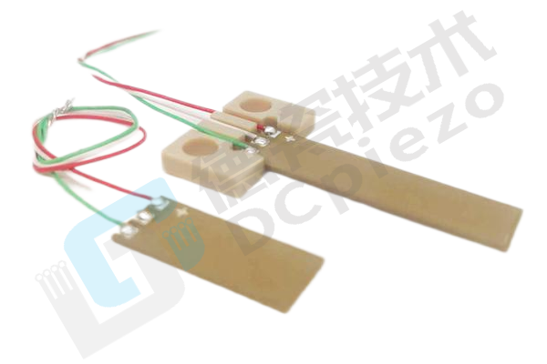
Multi-Layer Piezoelectric Bimorph
A high-sensitivity piezoelectric ceramic component operating in bending vibration mode, achieving large deflection displacement and superior energy conversion efficiency through innovative multi-layer piezoelectric-metal composite design. Its core structure combines alternating piezoelectric ceramic layers and elastic metal substrates, generating controlled bending deformation under electric field excitation. Capable of simultaneous actuation and sensing, it excels in acoustic transduction, precision micro-motion, and vibration energy harvesting. Widely applied in micro speakers, ultrasonic sensors, medical imaging probes, and smart touch devices, it delivers lightweight, high-responsiveness power solutions for advanced systems.
n, empowering technological upgrades in smart devices and precision systems.

Multi-Layer Piezoelectric Bimorph

Multi-Layer Piezoelectric Bimorph
Redefining bending deformation limits with innovative layered composite architecture and advanced materials, this component emerges as the optimal choice for miniaturized high-sensitivity actuation/sensing systems. As professional manufacturers, we ensure reliability and peak performance through stringent process control and scenario-specific customization, empowering technological upgrades in smart devices and precision systems.
Structural Design
● Multi-Layer Composite Architecture: Alternating piezoelectric ceramic and elastic metal layers with optimized polarization/field alignment to amplify bending deformation and force density.
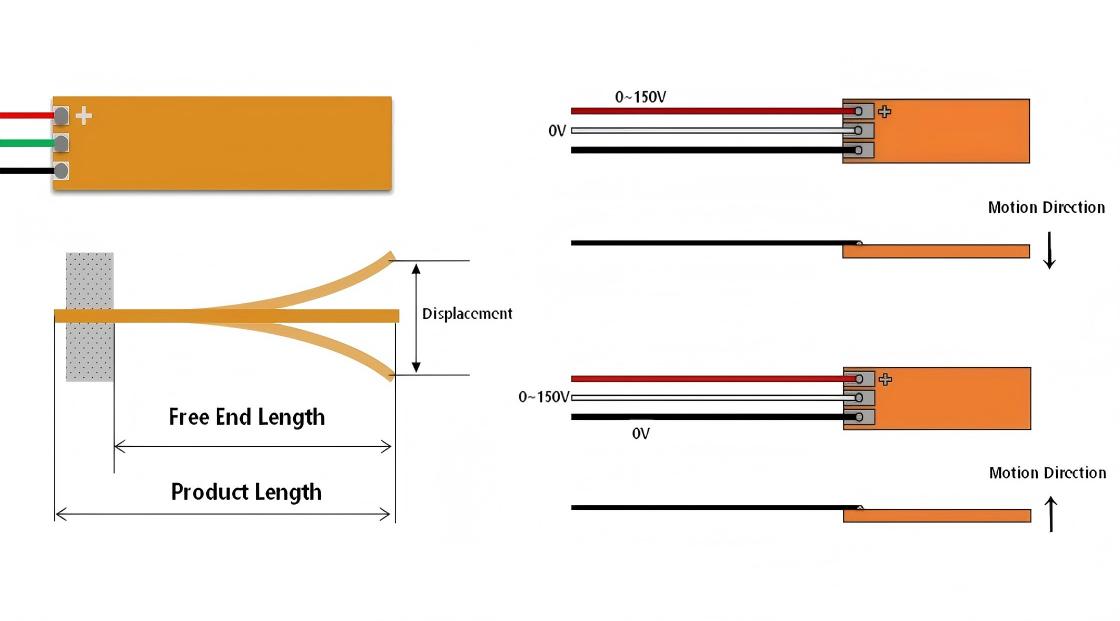
● Symmetrical Polarization: Oppositely polarized adjacent piezoelectric layers generate unidirectional bending under excitation, achieving millimeter-level displacement with reduced driving voltage.
● Lightweight Encapsulation: Ultra-thin epoxy/polyimide protective coating ensures flexibility and fatigue resistance, compatible with curved surfaces and high-frequency vibration environments.
Material Properties
● High-Sensitivity Piezoelectric Material: PZT-based composition with high d31 coefficient (≥320×10^-12 m/V), improving bending mode efficiency by 40%+.
● Enhanced Flexural Strength: Matched thermal expansion coefficients between metal/ceramic layers triple fracture resistance compared to single-layer bimorphs.
● Broadband Frequency Response: Adjustable resonance frequency (100Hz~50kHz) accommodates acoustic/ultrasonic multi-band applications.
Core Advantages
● Large Bending Displacement: 0.5~2mm free-end displacement under low voltage (≤50V), outperforming traditional single-layer bimorphs.
● High-Sensitivity Sensing: μN-level force detection with bidirectional energy conversion for self-powered sensing and energy harvesting.
● Rapid Dynamic Response: <1ms electromechanical response enables real-time haptic feedback and high-frequency acoustic emission.
● Robust Environmental Resistance: Moisture-proof, EMI-resistant, and operable at -25°C~130°C for industrial-grade reliability.
Typical Applications
● Acoustics: Micro-speaker diaphragm actuation, ANC headphone vibration units, ultrasonic atomizers.
● Smart Sensing: Force feedback modules for touchscreens, e-skin pressure sensors, vibration energy harvesters.
● Medical Devices: Portable ultrasound probes, endoscopic scanning actuators, respiratory monitors.
● Industrial Testing: NDT ultrasonic transducers, pipeline crack monitoring exciters.
● Consumer Electronics: OIS mechanisms for smartphone cameras, haptic alert modules in wearables.
Quality Commitment
● Full-Process QC: Monitored lamination strength and polarization uniformity from tape casting to sintering, with 100% bending fatigue and impedance testing.
● Customization Flexibility: Tailored dimensions, resonance frequencies, force/displacement curves, and encapsulation styles, including circuit impedance matching co-design.
● Lifecycle Support: Application simulation, installation guidance, failure analysis, and 24/7 technical consultation to ensure seamless integration and optimized performance.
