Square Piezoelectric Ceramic Chip
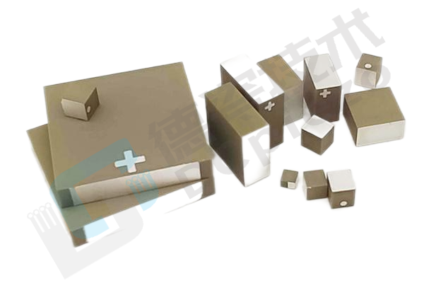
A high-performance multi-layer stacked piezoelectric core component designed for compact precision actuation and sensing. Featuring alternating ceramic and electrode layers, it enables low-voltage driving, rapid response, and high-accuracy displacement output. The chip integrates dozens to hundreds of ultra-thin piezoelectric layers with printed external electrodes and full-ceramic insulation on all sides, omitting a central bore to maximize structural integrity. Widely used in optical focusing, ultrasonic transduction, MEMS, and automation control, it delivers miniaturized, highly reliable electromechanical conversion for space-constrained applications.

Square Piezoelectric Ceramic Chip

Square Piezoelectric Ceramic Chip
Achieving optimal balance between low-voltage operation and precision control through multi-layer stacking innovation. As specialized manufacturers, we provide high-reliability, rapid-response core components via advanced materials and precision engineering, empowering breakthroughs in optical, ultrasonic, and automation technologies.
Structural Design
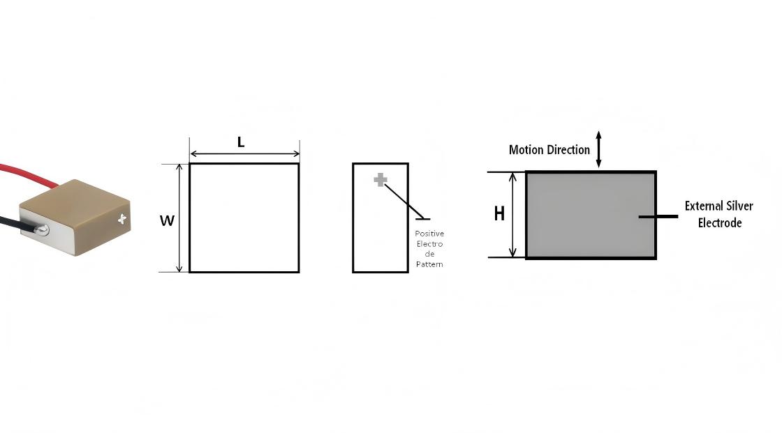
● Multi-Layer Cross Stacking: Ultra-thin piezoelectric ceramic layers alternating with internal electrodes, featuring printed external electrodes on both sides. Customizable stack thickness (standard: 2mm/3mm) with 0.1% thickness-to-displacement ratio and >99% linearity.
● Full-Seal Insulation: Dense ceramic insulation on all sides for moisture/leakage protection, with crosshair polarity markers to prevent installation errors.
● Bore-Free Compact Design: Solid structure enhances mechanical strength for high-load scenarios, supporting surface mounting or mechanical preload fixation.
● Interface Flexibility: Available as bare chips or pre-bonded with wires (Au/Cu) for soldering/spring-contact integration.
Material Properties
● High-Activity Piezoelectric Ceramic: Modified PZT-based material with d33≥500 pC/N and enhanced electromechanical coupling, improving energy efficiency by 40%+.
● Low-Impedance Electrodes: Ag-Pd alloy internal electrodes and Ag-printed external electrodes (resistivity <0.3Ω·cm) support wide voltage ranges (-30V~150V) and kHz-level responses.
● Precision Machining: Surface flatness <±5μm and roughness Ra<0.2μm ensure optimal contact and minimal energy loss.
Core Advantages
● Low-Voltage High-Output: Operates at reduced voltages (-10V~75V/-20V~100V/-30V~150V) with 150N/mm² force density, ideal for portable/low-power systems.
● Sub-Micron Precision: Nanometer-level resolution and <0.1% repeatability for ultra-precise positioning and micro-force control.
● Microsecond Response: <50μs electromechanical response enables high-frequency dynamics (ultrasonic vibration, fast valving).
● Environmental Robustness: Full-ceramic encapsulation withstands moisture/aging, operable at -25°C~130°C with >5×10^7 cycle life.
Typical Applications
● Optical Systems: Microscope objective focusing, laser cavity real-time length correction.
● Ultrasonic Tech: Ultrasonic cleaner transducers, NDT probes, medical imaging oscillators.
● Automation: Semiconductor bond head force feedback, robotic joint actuation.
● MEMS: Micro-sensor excitation, micropump diaphragm drives.
● Consumer Electronics: Smartphone camera OIS modules, haptic feedback units.
Quality Commitment
● Full-Process QC: Laser-monitored thickness/flatness from tape casting to sintering, 100% high-voltage polarization and displacement validation.
● Customization: Tailored thickness (1-10mm), voltage ranges, force/displacement curves, and wire bonding options, with prototypes in 7 business days.
● Technical Support: Driver circuit matching, installation stress simulation, dynamic optimization, and 24/7 consultation.
